Global 200mm Silicon Wafers Market Growth, Semiconductor Demand, and Mature Node Expansion
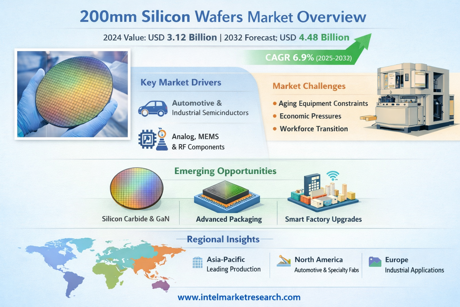
According to a new report from Intel Market Research, the global 200mm Silicon Wafers market was valued at USD 3.12 billion in 2024 and is projected to reach USD 4.48 billion by 2032, growing at a CAGR of 6.9% during the forecast period (2025-2032). This steady growth trajectory highlights the enduring importance of 200mm wafer technology in semiconductor manufacturing despite the industry's shift toward larger diameters.
📥 Download FREE Sample Report: 200mm Silicon Wafers Market - View in Detailed Research Report
What are 200mm Silicon Wafers?
200mm silicon wafers serve as the workhorse substrate for semiconductor manufacturing, offering the ideal balance between production economics and technological capability. These circular discs of ultra-pure silicon, measuring 200mm (8 inches) in diameter, form the foundation for fabricating integrated circuits used across countless electronic devices. While the semiconductor industry has largely transitioned to 300mm wafers for leading-edge logic processes, 200mm platforms continue to thrive for specialized applications where their mature, cost-effective manufacturing process provides significant advantages.
The resilience of the 200mm wafer market stems from its role in producing analog chips, power management ICs, MEMS sensors, and RF components — all essential for today's connected world. These wafer sizes remain particularly valuable for automotive semiconductors and industrial applications where reliability and established manufacturing processes outweigh the benefits of cutting-edge nodes. What makes 200mm wafers unique is their ability to support both conventional silicon-based devices and emerging materials like silicon carbide, creating versatile production platforms that bridge the past and future of semiconductor technology.
Key Market Drivers
Sustained Demand for Automotive and Industrial Semiconductors
The automotive sector's rapid transformation represents perhaps the strongest driver for 200mm wafer demand. Modern vehicles incorporate hundreds of semiconductors — from power management ICs to sensors — with most manufactured on mature process nodes. The shift toward electrification creates particularly robust demand for power devices, often produced most economically on 200mm platforms. Similarly, industrial automation and IoT deployments continue to drive steady orders for reliable, cost-effective chips made using established 200mm processes.
Limited Migration of Specialty Technologies
Many semiconductor applications simply don't benefit from migration to advanced nodes or larger wafer sizes. MEMS sensors, RF filters, and certain analog devices often rely on specialized processes that remain entrenched in 200mm fabs. The physics of these devices frequently require specific manufacturing approaches that are either technically challenging or economically unviable to transition to 300mm production. This creates enduring demand for 200mm capacity as these technologies experience their own growth trajectories in 5G, automotive, and medical applications.
Market Challenges
- Aging Equipment Constraints – The secondary market for 200mm fabrication tools has become increasingly constrained, with refurbished equipment commanding premium prices and long lead times. This creates operational challenges for fab operators needing to maintain or expand capacity.
- Economic Pressures – While demand remains strong, wafer prices face downward pressure as buyers seek to maximize the cost benefits of mature node production. This can squeeze margins for wafer suppliers and foundries alike.
- Workforce Transition – As younger engineers focus on advanced nodes, maintaining expertise in optimizing 200mm production lines becomes increasingly challenging, potentially impacting yields and innovation.
Emerging Opportunities
The future of 200mm wafer technology extends beyond simply maintaining legacy capacity. Several promising developments could extend the platform's relevance and create new growth avenues:
- Compound Semiconductor Integration – Adapting 200mm lines for silicon carbide and gallium nitride production offers a compelling path to more cost-effective power electronics manufacturing.
- Hybrid Manufacturing Models – Companies are finding success combining 200mm front-end processing with advanced packaging techniques, creating high-value solutions without requiring full migration to larger wafer sizes.
- Smart Factory Upgrades – Implementing Industry 4.0 technologies in 200mm fabs can significantly boost productivity and yields, making mature nodes more competitive.
Regional Market Insights
The Asia-Pacific region dominates 200mm wafer production and consumption, home to both leading suppliers like Shin-Etsu and SUMCO and major semiconductor manufacturers. Taiwan serves as the global hub for mature node foundry services, while China has made significant investments in domestic 200mm capacity. North America and Europe maintain important specialty manufacturing bases, particularly for automotive and industrial applications, though both regions face growing pressure to ensure supply chain resilience for mature node chips.
Competitive Landscape
The 200mm wafer market remains concentrated among established suppliers, with the top three companies controlling over 70% of global production capacity. This oligopolistic structure creates high barriers to entry given the technical expertise and capital requirements. However, regional players in China and South Korea are making strategic investments to build domestic supply chains, while foundries like TSMC and GlobalFoundries continue expanding 200mm capacity to meet sustained demand.
📘 Get Full Report Here: 200mm Silicon Wafers Market - View Detailed Research Report
About Intel Market Research
Intel Market Research is a leading provider of strategic intelligence, offering actionable insights in semiconductor manufacturing, electronics components, and industrial technologies. Our research capabilities include:
- Comprehensive market sizing and forecasting
- Supply chain and manufacturing analysis
- Technology trend assessment
- Competitive benchmarking and strategy evaluation
Trusted by technology leaders worldwide, our insights support decision-making across the semiconductor value chain.
🌐 Website: https://www.intelmarketresearch.com
📞 Asia-Pacific: +91 9169164321
🔗 LinkedIn: Follow Us