Wafer Used PVD Equipment Market to Reach USD 14.67 Billion by 2034, Fueled by Advanced Node Semiconductor Expansion
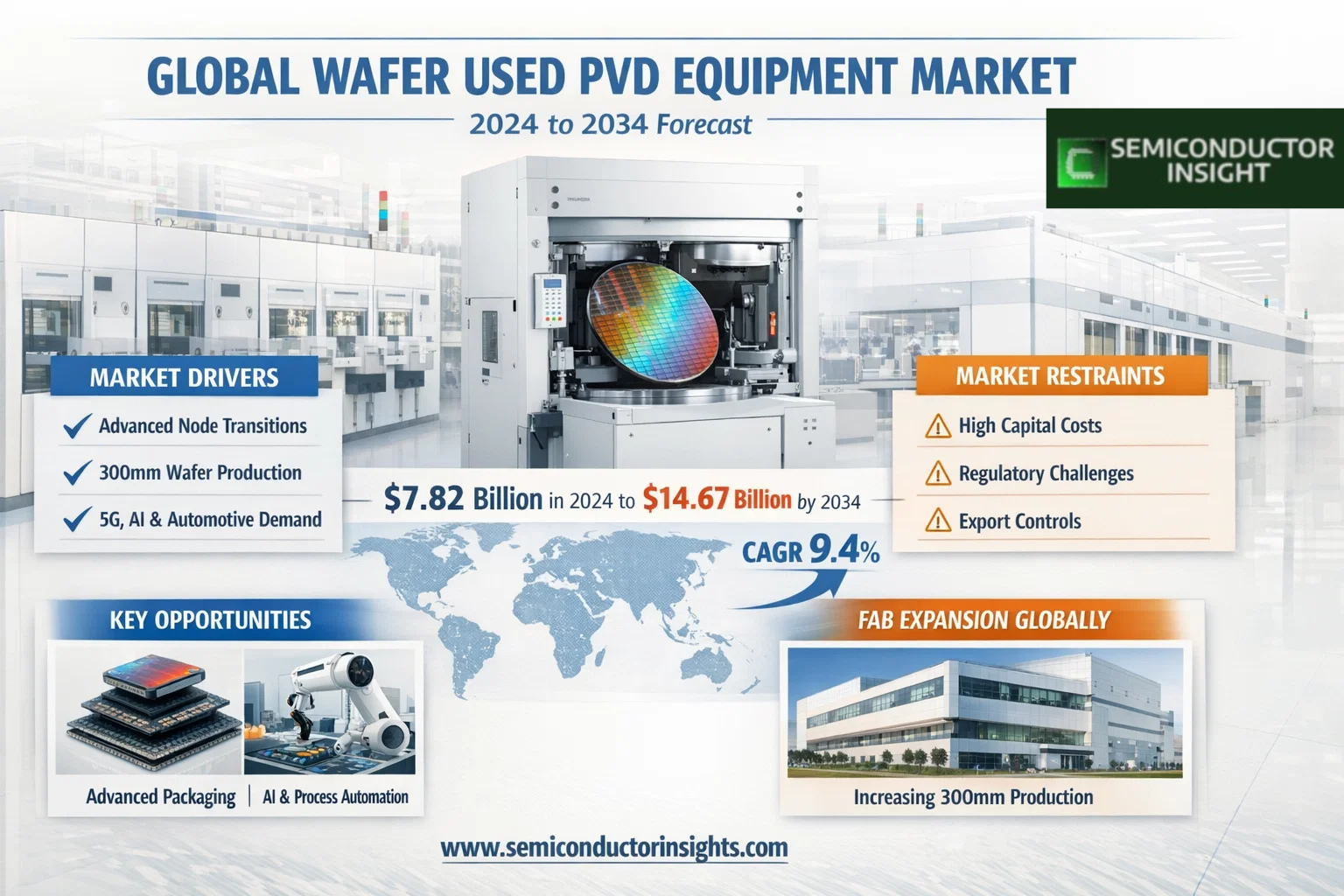
Global Wafer Used PVD Equipment market was valued at USD 7.82 billion in 2024 and is projected to reach USD 14.67 billion by 2034, expanding at a CAGR of 9.4% during the forecast period 2026–2034. The market is experiencing sustained growth as semiconductor manufacturers accelerate advanced node production and expand fabrication capacity worldwide.
Wafer used PVD (Physical Vapor Deposition) equipment refers to specialized semiconductor manufacturing systems designed to deposit ultra-thin film materials onto silicon wafers through sputtering or evaporation processes. These tools are essential for forming metal interconnects, diffusion barriers, seed layers, and dielectric films in advanced logic and memory devices. Key system variants include HardMask PVD for dielectric patterning layers, CuBS PVD for copper barrier and seed deposition, and AlPAD PVD for aluminum pad formation.
👉 Access the complete industry analysis and demand forecasts here:
https://semiconductorinsight.com/report/global-wafer-used-pvd-equipment-market/
Market Definition and Dynamics
The wafer PVD equipment market is closely linked to semiconductor capital expenditure cycles, advanced node transitions, and wafer size expansion toward 300mm high-volume production. Increasing demand from consumer electronics, automotive electronics, 5G infrastructure, AI accelerators, and IoT devices continues to drive fab expansions globally.
Market Drivers
- Rising global semiconductor demand driving new fab construction and capacity expansion
- Transition to sub-7nm and advanced nodes requiring ultra-thin, high-uniformity film deposition
- Government semiconductor subsidy programs accelerating capital equipment investments
- Growth in 300mm wafer production for high-volume logic and memory manufacturing
Market Restraints
- High capital expenditure requirements, with advanced cluster tools costing up to tens of millions per installation
- Regulatory and export control complexities affecting equipment deployment
- Extended ROI cycles limiting smaller manufacturer participation
Market Opportunities
- Expansion of advanced packaging and heterogeneous integration requiring TSV and redistribution layer deposition
- AI-driven process control and predictive maintenance creating recurring service revenue models
- Localization of semiconductor ecosystems supporting domestic equipment suppliers
Competitive Landscape
Major vendors continue investing heavily in R&D to support advanced barrier materials, high-aspect-ratio deposition, and hybrid ALD-PVD system integration to maintain technological leadership.
List of Key Wafer Used PVD Equipment Companies
- Applied Materials, Inc.
- Ulvac Technologies, Inc.
- KLA Corporation
- NAURA Technology Group Co., Ltd.
- Evatec AG
- Canon Anelva Corporation
- Tokyo Electron Limited
- Veeco Instruments Inc.
- Plasma-Therm LLC
Segment Analysis
By Type
- HardMask PVD Equipment
- CuBS PVD Equipment
- AlPAD PVD Equipment
- Others
By Application
- IDM (Integrated Device Manufacturers)
- Foundry
- Others
By Technology
- Sputtering
- Evaporation
- Others
By Wafer Size
- 200mm
- 300mm
- Others
Regional Insights
Asia-Pacific accounts for the largest share of global demand, driven by major semiconductor manufacturing hubs in Taiwan, South Korea, China, and Japan. The region benefits from large-scale foundry expansions and government-backed semiconductor initiatives. North America remains a key innovation hub supported by significant CHIPS Act funding and advanced logic manufacturing investments. Europe focuses on specialty semiconductor applications, particularly automotive and industrial chips, supported by regional Chips Act initiatives. South America and the Middle East & Africa represent emerging markets, primarily centered on packaging, testing, and niche semiconductor applications with gradual infrastructure development.
👉 Access the complete industry analysis and demand forecasts here:
https://semiconductorinsight.com/report/global-wafer-used-pvd-equipment-market/
📄 Download a free sample to explore segment dynamics and competitive positioning:
https://semiconductorinsight.com/download-sample-report/?product_id=95961
About Semiconductor Insight
Semiconductor Insight is a global intelligence platform delivering data-driven market insights, technology analysis, and competitive intelligence across the semiconductor and advanced electronics ecosystem. Our reports support OEMs, investors, policymakers, and industry leaders in identifying high-growth markets and strategic opportunities shaping the future of electronics.
🌐 https://semiconductorinsight.com
🔗 LinkedIn: Follow Us https://www.linkedin.com/company/semiconductor-insight/
📞 International Support: +91 8087 99 2013