Semiconductor Packaging Materials Market to Reach USD 68.9 Billion by 2034 Driven by Advanced Packaging Technologies
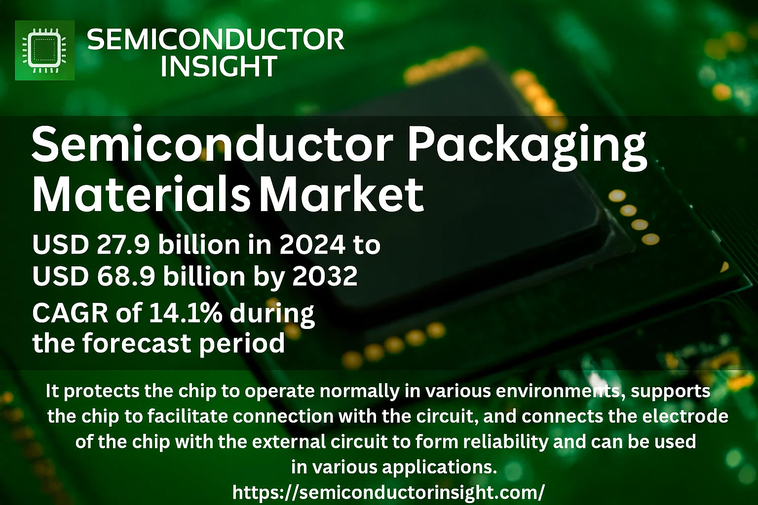
global Semiconductor Packaging Materials Market was valued at USD 27.9 billion in 2024 and is projected to reach USD 68.9 billion by 2032, registering a CAGR of 14.1% during the forecast period 2025–2032. Market expansion is fueled by the rapid growth of advanced electronics, increasing adoption of artificial intelligence (AI), Internet of Things (IoT), high-performance computing, and the growing semiconductor demand in automotive and electric vehicle applications.
Semiconductor packaging materials play a critical role in the protection, support, electrical connection, and reliability of semiconductor chips. These materials enable chips to function effectively in diverse operating environments by protecting sensitive circuits, supporting mechanical structure, and ensuring efficient connectivity between the chip and external circuits. As semiconductor devices become smaller and more powerful, advanced packaging materials are essential to maintain thermal management, signal integrity, and long-term reliability.
👉 Access the full report and detailed market insights:
https://semiconductorinsight.com/report/semiconductor-packaging-materials-market/
Market Overview
The semiconductor industry is undergoing a major transformation driven by emerging technologies such as artificial intelligence, cloud computing, 5G connectivity, and autonomous vehicles. These developments require high-performance semiconductor devices, which in turn depend heavily on advanced packaging technologies.
Packaging materials are fundamental components in semiconductor manufacturing, supporting packaging platforms such as flip-chip, wafer-level packaging, and 2.5D/3D integration. These technologies enable higher performance, improved thermal efficiency, and greater device miniaturization.
The increasing global demand for consumer electronics, data center infrastructure, and electric vehicles is significantly contributing to the expansion of the semiconductor packaging materials market. For example, the global electric vehicle market is expected to reach approximately 26.9 million units by 2030, driving higher semiconductor usage and packaging material demand.
Market Drivers
Proliferation of Advanced Electronics and Miniaturization
The continuous demand for smaller, faster, and more powerful electronic devices is accelerating the adoption of advanced semiconductor packaging technologies. Packaging platforms such as fan-out wafer-level packaging (FOWLP) and 2.5D/3D integration require highly specialized materials including advanced substrates, encapsulants, and thermal interface materials.
Rapid Growth in Automotive Electronics and High-Performance Computing
The electrification of vehicles, the adoption of advanced driver-assistance systems (ADAS), and the rapid expansion of AI data centers are driving demand for packaging materials capable of operating under high temperature and high-performance environments.
Expansion of IoT and 5G Infrastructure
The growing deployment of IoT devices and 5G networks requires compact and cost-efficient semiconductor packaging solutions, accelerating the demand for advanced lead frames, epoxy molding compounds, and bonding materials.
Market Restraints
High Capital Investment for Advanced Material Development
Developing next-generation semiconductor packaging materials requires significant R&D investment and advanced manufacturing infrastructure, creating barriers for smaller market participants.
Cyclicality of the Semiconductor Industry
The semiconductor market experiences periodic demand fluctuations, which directly influence production volumes and packaging material demand.
Market Challenges
Supply Chain and Raw Material Cost Volatility
Packaging materials rely on high-purity metals, specialty resins, and ceramics. Price volatility and geopolitical disruptions can impact supply stability and production costs.
Increasing Technical Complexity
As semiconductor nodes shrink to 5nm and below, packaging materials must meet strict requirements for dielectric performance, thermal expansion control, and signal reliability.
Environmental and Regulatory Compliance
Global regulations such as RoHS and REACH require manufacturers to develop environmentally friendly materials, increasing development costs and technical complexity.
Market Opportunities
Emerging High-Performance Computing Applications
AI processors, quantum computing, and advanced GPUs require packaging materials with exceptional thermal and electrical performance, creating new opportunities for innovative material solutions.
Sustainable Semiconductor Materials
Growing sustainability goals are encouraging the development of eco-friendly packaging materials such as bio-based encapsulants and recyclable substrates.
Adoption of Chiplet Architecture
Chiplet-based semiconductor designs are driving demand for specialized interconnect materials, advanced substrates, and high-density packaging technologies.
Competitive Landscape
The Semiconductor Packaging Materials Market is moderately concentrated, with leading Japanese and Asian manufacturers holding a significant share. Companies such as Kyocera, Shinko, and Ibiden collectively account for more than 22% of the global market.
These companies maintain competitive advantages through strong R&D capabilities, advanced manufacturing technologies, and long-term partnerships with semiconductor foundries and integrated device manufacturers.
Major suppliers across different packaging material segments include substrate manufacturers, bonding wire providers, encapsulation specialists, and adhesive solution providers.
Key Semiconductor Packaging Materials Companies
- Kyocera
- Shinko
- Ibiden
- LG Innotek
- Unimicron Technology
- ZhenDing Tech
- Semco
- KINSUS Interconnect Technology
- Nan Ya PCB
- Nippon Micrometal Corporation
- Simmtech
- Mitsui High-tec
- HAESUNG
- Shin-Etsu
- Heraeus
- Henkel
Market Segmentation
By Type
- Packaging Substrate
- Lead Frame
- Bonding Wire
- Encapsulating Resin
- Ceramic Packaging Material
- Chip Bonding Material
- Others
By Application
- Consumer Electronics
- Automobiles
- Communications
- Medical
- Others
By End User
- Semiconductor Foundries
- Integrated Device Manufacturers (IDMs)
- Outsourced Semiconductor Assembly and Test (OSAT)
By Material Technology
- Organic Substrates
- Ceramic Packages
- Advanced Encapsulants
By Packaging Platform
- Flip-Chip
- Wafer-Level Packaging (WLP)
- 3D / 2.5D IC Integration
Regional Insights
Asia-Pacific
Asia-Pacific dominates the global semiconductor packaging materials market due to the presence of leading semiconductor manufacturing hubs in Taiwan, South Korea, China, and Japan. The region hosts a high concentration of OSAT providers, semiconductor foundries, and integrated device manufacturers, creating strong demand for advanced packaging materials.
North America
North America remains a major innovation hub with strong demand driven by AI processors, high-performance computing, and advanced semiconductor research. The region focuses on developing high-value packaging materials for next-generation computing applications.
Europe
Europe’s market growth is supported by strong automotive electronics demand and strict reliability requirements for industrial and medical semiconductor applications.
Latin America and Middle East & Africa
These regions represent emerging markets where semiconductor packaging demand is gradually increasing due to expanding electronics manufacturing and technology investments.
📄 Download the free sample report here:
https://semiconductorinsight.com/download-sample-report/?product_id=90973
About Semiconductor Insight
Semiconductor Insight is a global intelligence platform delivering data-driven market insights, technology analysis, and competitive intelligence across the semiconductor and advanced electronics ecosystem. Our reports support OEMs, investors, policymakers, and industry leaders in identifying high-growth markets and strategic opportunities shaping the future of electronics.
🌐 https://semiconductorinsight.com
🔗 LinkedIn: Follow Us
https://www.linkedin.com/company/semiconductor-insight/
📞 International Support: +91 8087 99 2013